

Introduction to Wide-Bandgap Semiconductors
Table of Contents
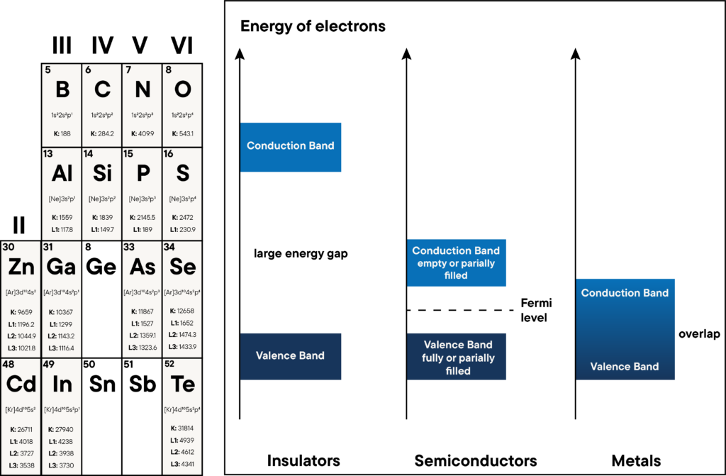
Semiconductors with an energy gap (Eg) larger than conventional semiconductors, typically in the range above 2eV, are termed as wide-bandgap semiconductors (WbG’s).
In comparison, the commonly used semiconductors Si and GaAs have a andgap of 1,1 eV and 1,43 eV, respectively. They developed because semiconductor technology needed to be extended to optical manipulation and high-power and high-frequency devices.
Most of the WBGS’s are essentially known for their structure and unique properties. Various growth techniques have been developed to synthesize materials with excellent properties, low defect concentration, and good control of their stoichiometry.
WBGS’s have electronic properties that fall in between those of conventional semiconductors and insulators, allowing them to operate at much higher voltages, frequencies, and temperatures than conventional semiconductor materials like silicon and gallium arsenide.
WBGS’s are used in a wide range of applications, including short-wavelength (green to UV) LEDs or lasers, military radars, and certain radio frequency applications.
Their high temperature tolerance makes them highly attractive for military applications, and they are also used in power conversion applications, where they can handle higher power levels under normal operating conditions.
Furthermore, WBGS’s can be used in solid-state lighting, where they have the potential to reduce the amount of energy required to provide lighting with a luminous efficacy of less than 20 lumens per watt.
The efficacy of LEDs using WBGS’s is on the order of 160 lumens per watt.
The energy gap of WBGS’s can be tailored with high bandgaps group III (Al, Ga, In) and V (N, P, As, Sb) atoms. Formation of III–V ternary and quaternary alloys and II-VI compound semiconductors.
The wider bandgap and thus the reduced thermal generation of charge carriers, allows WBGS’s to operate at much higher temperatures, e.g. up to 300°C or even 900°C.
The high breakdown voltage and high drift velocity enable it to operate at high switching frequencies (>20 kHz) and higher voltages and currents compared to conventional semiconductors.
The most common WBG materials include diamond and silicon carbide (SiC) and are the primary choice for high-power devices.
These materials are used in a variety of applications, including high-temperature and power switching applications, solid-state lighting, and radio frequency (RF) signal processing.
WBGS’s also have high free-electron velocities, which allows them to work at higher switching speeds, making them valuable in radio applications.
A single WBG device can be used to make a complete radio system, eliminating the need for separate signal and radio-frequency components, while operating at higher frequencies and power levels.
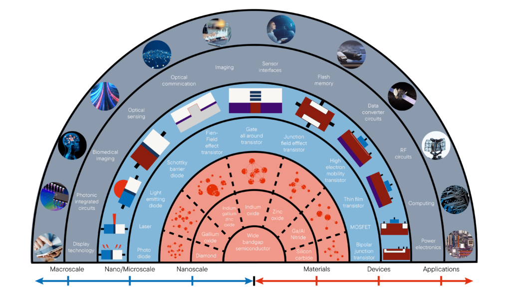
WBGS’s are applied in numerous electronic and optoelectronic domains (Fig. 2).
Applications of Wide-Bandgap Semiconductors
Electronic Applications of Wide-Bandgap Semiconductors
- Power electronics:
- wide-bandgap devices enable higher energy efficiency, power density, and higher operating temperatures in converters, inverters, and motor drives.
- Computing:
- high-speed switching capabilities of wide-bandgap transistors enhance computing performance.
- RF circuits:
- high-frequency operation and efficient power handling are essential for wireless communication systems.
- Data converter circuits:
- enhanced speed and precision of analog-to digital and digital-to-analog converters.
- Flash memory:
- wide-bandgap memory devices exhibit faster read and write speeds, longer lifespan, and lower power consumption.
- Sensor interfaces:
- wide-bandgap devices improve sensor sensitivity and interface capabilities.
Optoelectronic Applications of Wide-Bandgap Semiconductors
- Imaging:
- wide-bandgap devices enable high-resolution and high sensitivity imaging systems for scientific, medical, and industrial applications.
- Optical communication:
- high-speed, efficient optical devices are vital for data transmission in modern communication networks.
- Optical sensing:
- wide-bandgap photodetectors provide accurate and reliable sensing solutions for environmental and industrial monitoring.
- Data converter circuits:
- enhanced speed and precision of analog-to digital and digital-to-analog converters.
- Biomedical imaging:
- high-quality imaging devices contribute to advances in medical diagnostics and researches.
- Photonic integrated circuits:
- wide-bandgap materials enable compact and efficient photonic circuits for data processing and communication.
- Display technology:
- energy-efficient displays with improved colour accuracy and resolution are achieved with the adoption of wide bandgap devices.
Tailoring Energy Gap and Material Choices
There are more WBG material-based implementations more than the traditional silicon-based counterparts.
Some of the applications in addition to those illustrated in above fig are: solar power solutions, single-phase string inverters, three-phase string inverters, harnessing the wind power, auxiliary power, core power, hot-swap, server rack power.
Some other applications are transportation electrification solutions like electric vehicle (EV) auxiliary power, traction inverters, EV charging, starter generator, and onboard charger.
Thermal Analysis Techniques and Instruments
The thermal analysis techniques are crucial for understanding the thermal behaviour of WBG materials and ensuring their optimal performance in electronic devices.
They enable researchers and engineers to develop and optimize WBG devices for various applications, such as power electronics, RF and power devices, and batteries.
Thermal analysis techniques used for WBGS’s analysis include:
- Thermal resistance measurement
- Thermal conductivity measurement
- Thermal boundary resistance measurement
- Thermal management and packaging
Linseis Thermal Analysis offers a range of instruments for the WBGS’s analysis for thermal conductivity/resistivity, and the analysis of thermoelectric materials.
These instruments are designed for materials analysis in research and quality control, and are used in various industries such as chemical, automotive, polymer, and electronics.
Some of the specific thermal analysis products by Linseis include:
- Thermal Conductivity analyzer:
- These instruments measure heat transfer properties like thermal conductivity, thermal diffusivity or also the specific heat capacity, giving information about a WBGS’s ability to store and transfer heat or temperature. Linseis has a wide range of thermal conductivity instruments for the investigation of WBGS’s, such as:
- Laser Flash Analyzer (LFA) and the Transient Hot Bridge (THB) method allowing the determination of thermal diffusivity, thermal conductivity and specific heat capacity determination with high accuracy.
- The Thin Film Laser Frequency Analyzer (TF-LFA) and Thin Film Analyzer (TFA) are designed for measuring the thermal diffusivity and thermal conductivity of thin films in the µm to nm range, which are e.g. commonly used in the computational industries.
- These instruments measure heat transfer properties like thermal conductivity, thermal diffusivity or also the specific heat capacity, giving information about a WBGS’s ability to store and transfer heat or temperature. Linseis has a wide range of thermal conductivity instruments for the investigation of WBGS’s, such as:
- Thermoelectric analyzer: These devices measure the electric resistivity, Seebeck coefficient, ZT value and Hall coefficient and thus provide information about their electrical conductivity, charge carrier concentration and mobility. To these test devices belong the Linseis LSR-1 (LSR L32), LSR-3 (LSR L31) (Linseis Seebeck and resistivity meters) and HCS series (Hall Characterization System).
Summary and Conclusion
In summary, WBGS’s have often high free-electron velocities, which can significantly affect the performance of electronic devices. The wider bandgap enables them to operate at higher voltages, frequencies, and temperatures, while also handling higher power levels under normal operating conditions.
They are highly valuable in a wide range of applications, including military, radio, power conversion, and solid-state lighting.
Citations:
- Josh Perry, Cooling Wide-Bandgap Materials in Power Electronics June 15, 2018.
- Saravanan Yuvaraja, Vishal Khandelwal, Xiao Tang & Xiaohang Li, Wide bandgap semiconductor based
integrated circuits. Chip 2, 100072 (2023). - Maria Katsikini, Wide Band Gap Materials, X-Ray Absorption Spectroscopy of Semiconductors, 2015, Volume 190. ISBN: 978-3-662-44361-3.
- Yuan Qin, etal. Thermal management and packaging of wide and ultra-wide bandgap power devices: a review and perspective J. Phys. D: Appl. Phys. 56 (2023) 093001 (23pp).
- Anushree Ramanath- a technical article on Applications of Wide Bandgap Devices December 30, 2021.
