


Precise knowledge of the physical properties of thin films is becoming increasingly important in many branches of industry and applications.
Typical examples are phase change materials, optical storage media, thermoelectric materials, light emitting diodes (LEDs), fuel cells, phase change memories, flat screens and the semiconductor industry in general.
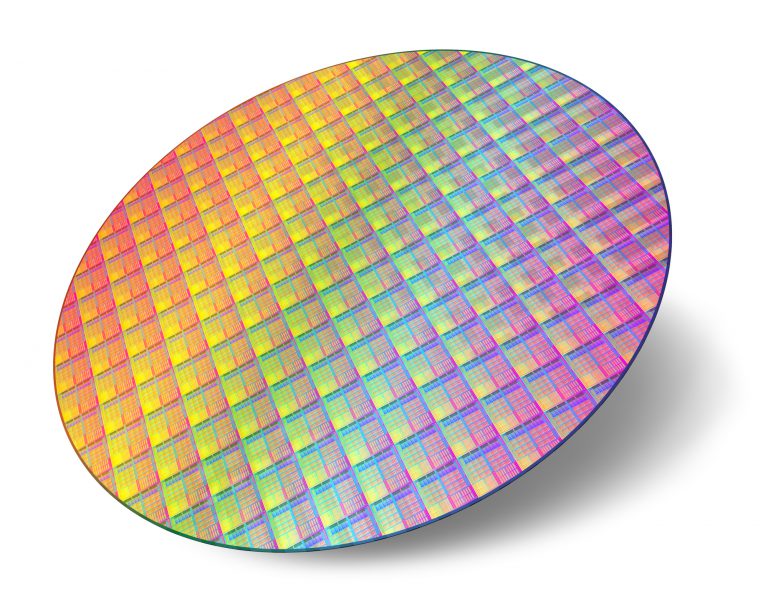
All these industries use single or multi-layer systems to give a device (or an assembly) a specific function.
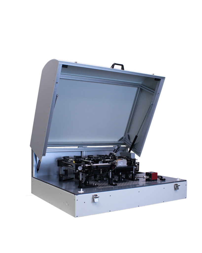
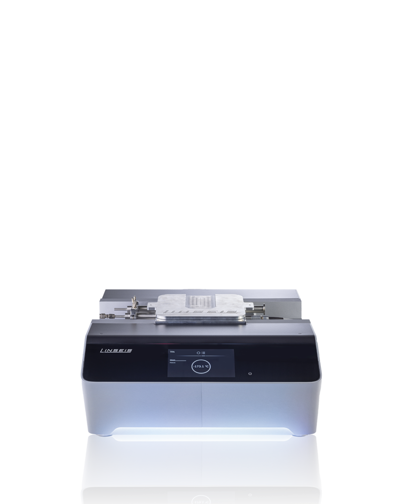
Since the physical properties of thin layers differ significantly from those of solid materials, it is necessary to determine their thickness and temperature-dependent properties using suitable measuring devices.
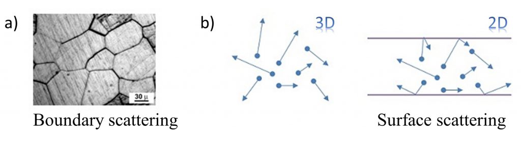
This is because large aspect ratios (layer thickness to lateral expansion) often result in additional boundary and surface scattering effects, which often lead to significantly reduced charge and heat transport.
Furthermore, there is a wide range of deposition technologies for producing thin films, which also have a major influence on the material properties of the thin film.
As the requirements for characterizing a thin film and a solid material differ significantly in some cases, different measurement techniques must be used for the two areas.
The thermal conductivity and electrical conductivity of thin films are usually lower than those of comparable solid materials.
For example, the thermal conductivity lambda of a 20 nm Si film or nanowire at room temperature can be a factor of five lower [1] than its solid, monocrystalline counterpart.
For a 100 nm thick gold film, it has also been shown that the electrical and thermal conductivity is also almost halved [2].
In general, it can be said that the transport properties are not only dependent on temperature, but also strongly on thickness [3].
Such reductions in conductivity can generally be attributed to two original causes.
On the one hand, the thin-film synthesis technology used often results in larger impurities and defects in a thin film, which lead to more disorder and grain boundaries within the material, which in turn leads to more scattering and thus reduced thermal conductivity and electrical conductivity.
In addition, even an atomically perfect thin film would be expected to have reduced thermal conductivity due to interfacial scattering and phonon leakage.
However, the two mechanisms influence the in-plane and cross-plane transport differently, so that the transport properties of thin films usually show anisotropic behavior.
This effect could be observed even if the corresponding solid material exhibits isotropic behavior.
[1] Li, Deyu, et al.
“Thermal conductivity of individual silicon nanowires.” Applied Physics Letters 83.14 (2003): 2934-2936.
[2] Linseis, V., Völklein, F., Reith, H., Nielsch, K., and Woias, P. 2018.
Thermoelectric properties of Au and Ti nanofilms, characterized with a novel measurement platform. Materials Today: Proceedings, ECT2017 Conference Proceedings.
[3] Linseis, V., Völklein, F., Reith, H., Hühne, R., Schnatmann, L., Nielsch, K., and Woias, P. 2018.
Thickness and temperature dependent thermoelectric properties of Bi87Sb13 nanofilms measured with a novel measurement platform. Semiconductor Science and Technology.